Impact of DC fault blocking capability on the sizing of the DC-DC Modular Multilevel Converter
This paper analyzes the impact on the converter design of including such characteristic for the DC-DC Modular Multilevel Converter.
This paper analyzes the impact on the converter design of including such characteristic for the DC-DC Modular Multilevel Converter.
A novel model and a multi-variable linear control for power and magnetizing average currents are proposed
In this prototype, achieving full operation was prevented by false triggering of semiconductors due to large common-mode current through gate drivers.
Simulation results of a MMC model and figures of merit are shown to provide consistent result, proving that the proposed figures of merit are a very simple and fast way to select the best semiconductor switch.
This paper introduces a unidirectional MVDC-HVDC converter for ‘all DC’ connected offshore wind farms.
This paper investigates the gate-driver design challenges encountered due to the fast switching of wide band-gap semiconductors (here, SiC MOSFETs) in the half-bridge configuration.
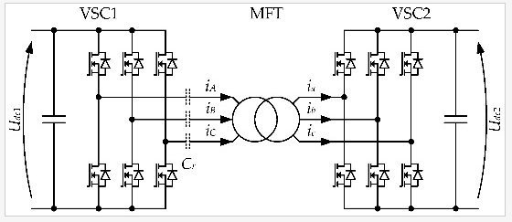
The experimental studies show the effects of the transformer construction and vector group (star/delta) on the common-mode currents through the gate drivers of SiC MOSFETs in a 100kW 1.2kV three-phase dual active bridge converter.
In this paper, a methodology is proposed to define the optimal rated power and number of PEBBs.
This article presents the measurements of the equivalent B(H) and the equivalent magnetic permeability of two three-phase MFT prototypes.
The work of this thesis focuses on the experimental development of a passive and biphasic cooling system to cool down power electronics. Some of those modules are mean voltage power converters developed by Supergrid Institute. Some constraints have been imposed upstream to this project. While some limitations are of the technological nature, other constraints are related mainly to the environmental and biological aspects. The first part of this thesis was to find a suitable cooling system that could be adapted to the project specifications. After some research, we decided to build a loop thermosiphon filled with NOVEC 649.