Thesis Ilyas DCHAR
“Design of a “fail-to-short” power module for HVDC applications”
Objective of the study
High Voltage Direct Current (HVDC) converters are composed of hundreds of semiconductor switches connected in series to sustain the rated voltage of the converter (several hundred of kilovolts). Because of the large number of switches, it is highly probable that at least one of them will fail during the lifetime of the converter. Such failure should not cause the entire converter to shut down, despite the series connexion of the switches. As a consequence, each switch should be designed so that upon failure, it becomes a short circuit and keeps carrying the current (“fail-to-short” behaviour).
Such fail-to-short switches are available on the market for silicon transistors. They rely on the melting of the silicon chips during the failure to form a conductive path. However, the new generation of high voltage semiconductors is based on silicon carbide (SiC), a material with very unique physical properties. The behaviour of SiC during failure must therefore be investigated.
Failure behaviour of SiC devices

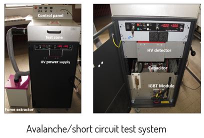
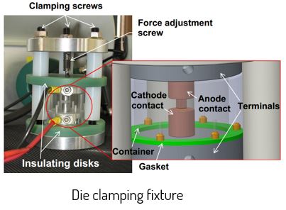
A test system was specifically designed for this study (photo). It allows testing of single-chip components in avalanche conditions (over-voltage, up to 3000V) and short-circuit conditions (over current, up to 2000 A). A clamping fixture (photo) was also designed to host SiC dies (diodes). With this fixture, various pieces of metallic foil can be placed in contact with the die to assess the behaviour during the failure test.

The energy leading to the failure of the die is recorded (we tested failure energies in the range 0.5-10 J), and the anode-cathode resistance is measured (a fail-to-short device should produce a very low resistance).
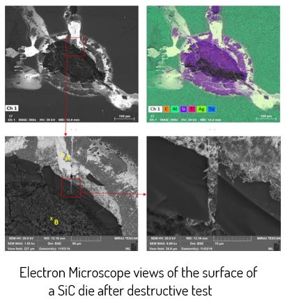
The surface of the die is also inspected using an electron microscope (photo). It is found that the failure produces craters at the surface of the die, but no melting of the SiC is observed (as it is the case with silicon dies). Only thin metal filaments can be seen (light grey areas on the photograph). However, these filaments are sufficient to produce a low resistance (in the order of 100 mOhms).

Conclusions
As expected, SiC dies do not melt during failure. This is a major difference with silicon. However, the shattering of the die and the evaporation of the surrounding metals which occur during failure are sufficient to form conductive paths, providing the package is robust enough (standard packages were found to explode, resulting in an open-circuit).
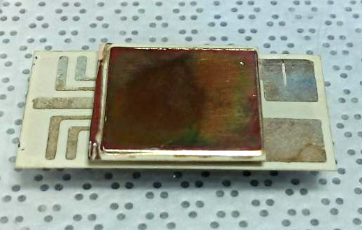
This was demonstrated ion a multi-chip package (photo), developed during the course of the project. This package contains two SiC 50A MOSFETs, with a “sandwich” structure which allows cooling on both sides of the package.

To go further
This work received an award at APEC.
Some of the publications (more to come):


